![]() |
![]() |
The PCBs. The ones I sell do not have the part#'s on them - hopefully I will take another picture soon... |
The
main board schematic. Because it's so derivative of several well known
designs (Mutable Links, MFOS Control Voltage Distributors #1 and #2)
and honestly most basic op-amp multiple designs, consider it licensed
with creative commons CC-BY-SA-3.0 license and do as thou wilt. |
Jack board schematic. |
MAIN BOARD BOM 
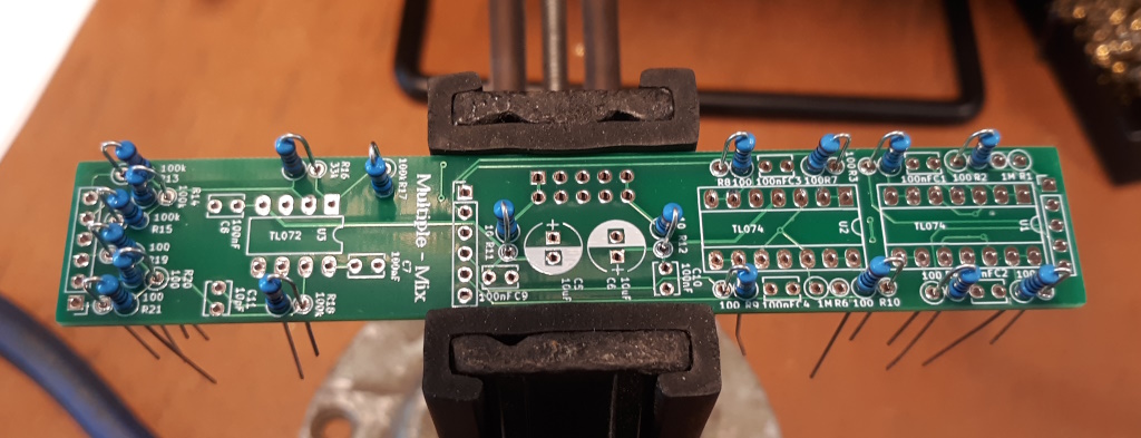
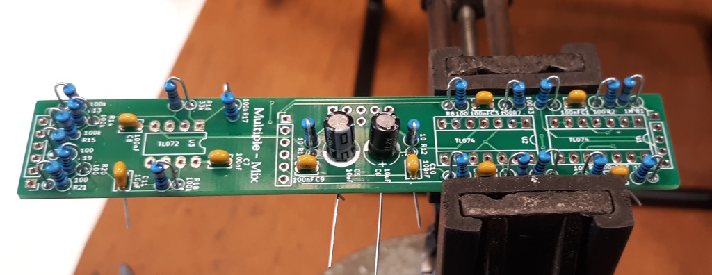
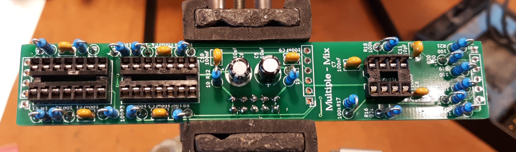
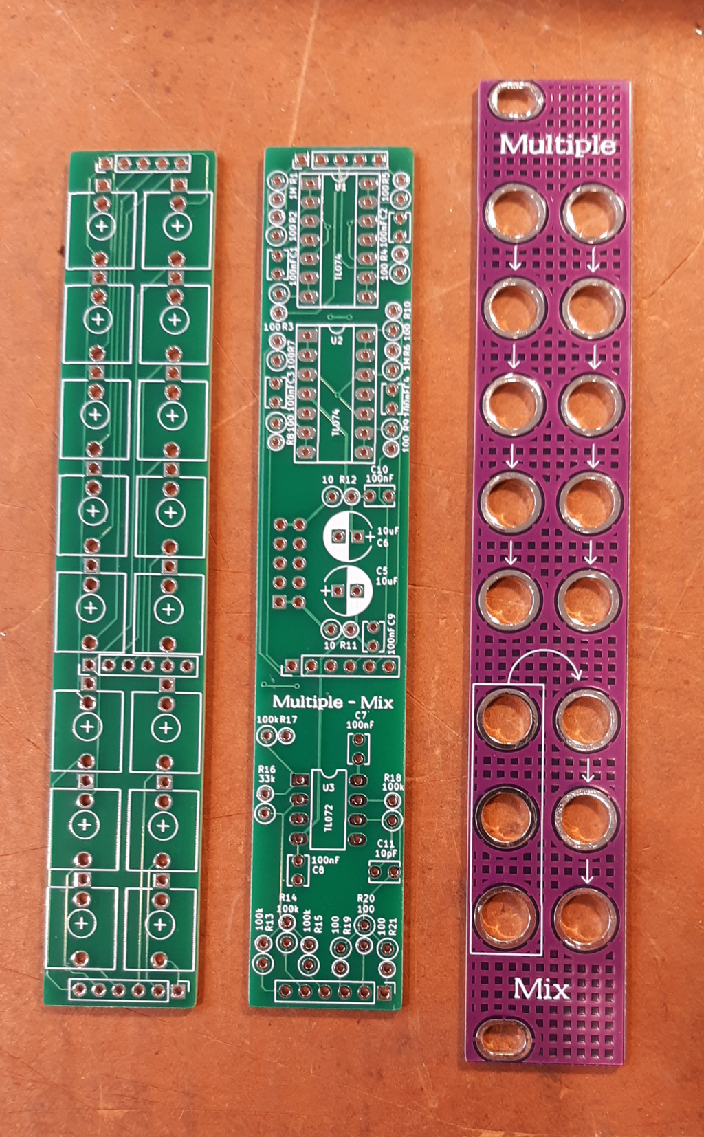
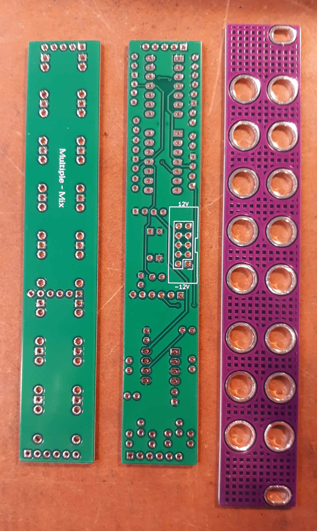
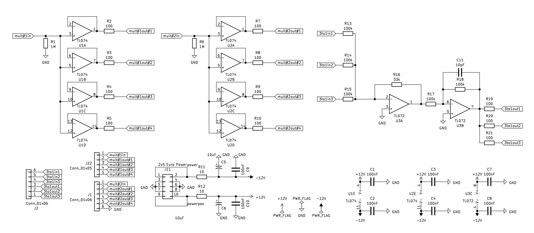
Qty Reference(s) Description 1 C11 10pF MLCC capacitor 2.5mm lead 8 C1, C2, C3, C4, C7, C8, C9, C10 100nF MLCC capacitor 2.5mm lead 
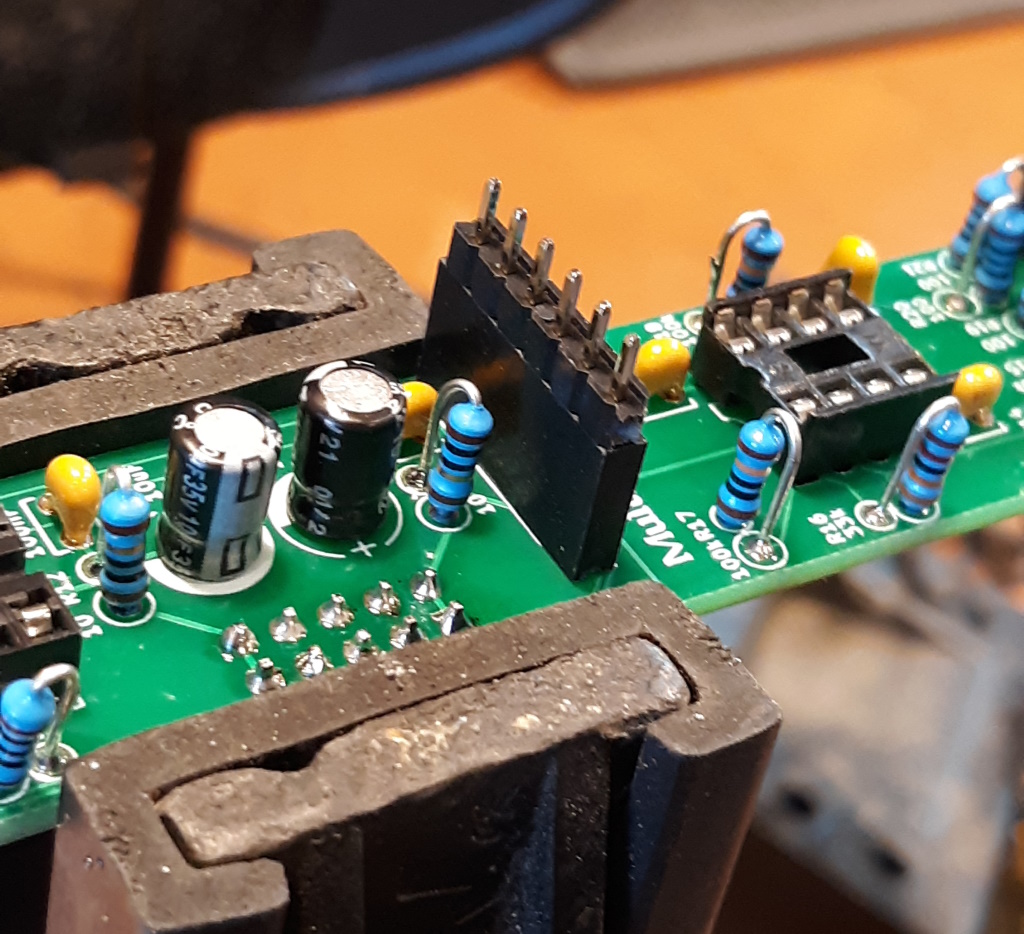
2 C5, C6 10uF Electronlytic Capacitor 2.5mm lead. Less than 11mm, best 10mm or shorter. 2 R11, R12 10 Ohm resistor, 1/4W Metal Film 1% (*see note below*) 
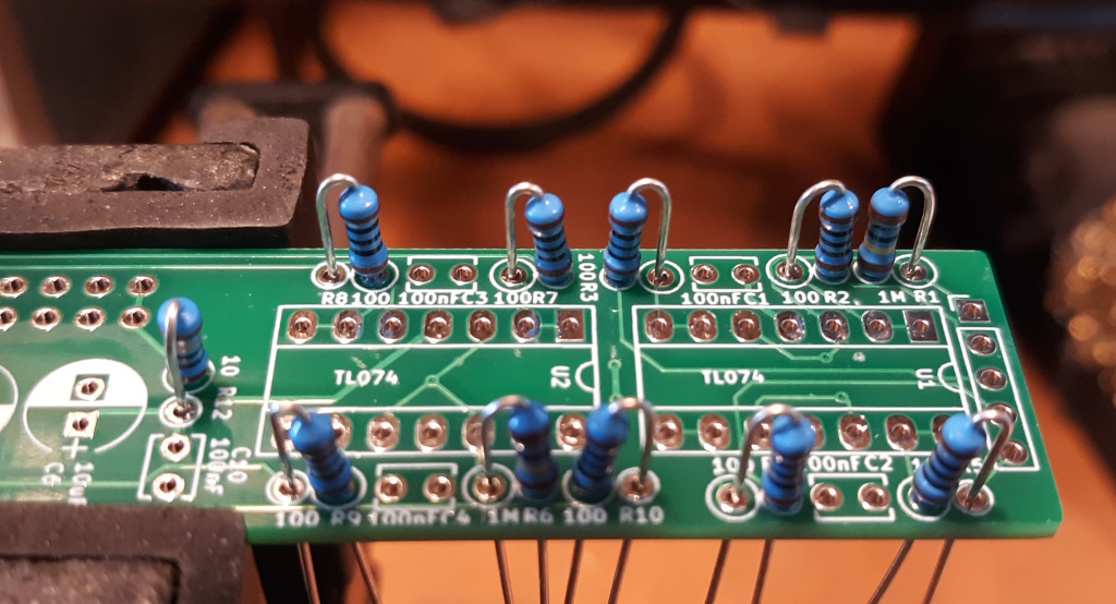
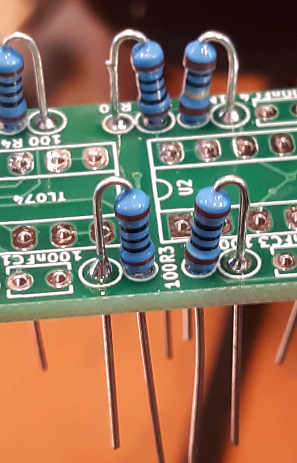
11 R2, R3, R4, R5, R7, R8, R9, 100 Ohm resistor, 1/4W Metal Film 1% R10, R19, R20, R21 1 R16 33K Ohm resistor, 1/4W Metal Film 1% 5 R13, R14, R15, R17, R18 100K Ohm resistor, 1/4W Metal Film 1% 2 R1, R6 1M Ohm resistor, 1/4W Metal Film 1% 
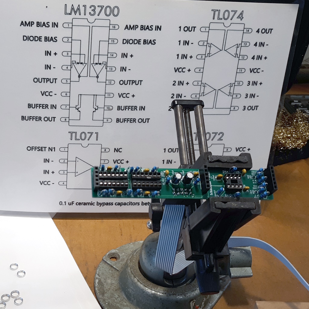
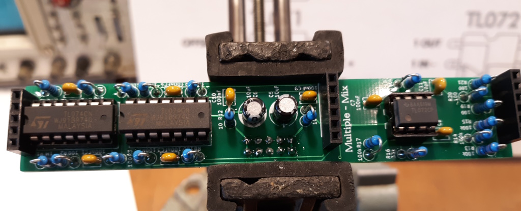
2 U1, U2 TL074 DIP package (use socket) 1 U3 TL072 DIP package (use socket) 3 U1,U2 DIP 14 Socket 1 U3 DIP 8 socket 
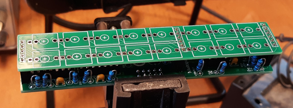
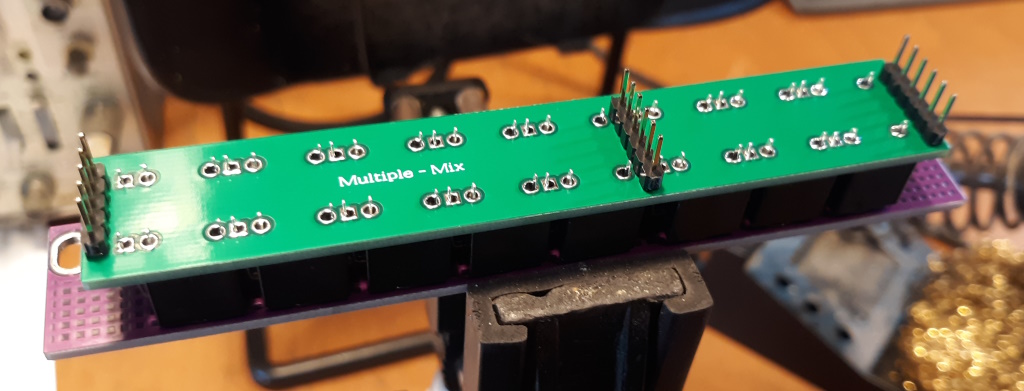
2 J1, J2 Female 1x6 header, 2.54mm pitch 1 J11 Male 2x5 shrouded header, 2.54 pitch 1 J22 Female 1x5 header, 2.54mm pitch
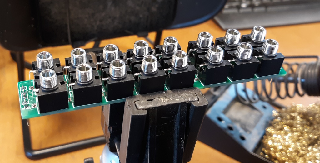
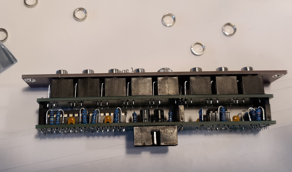
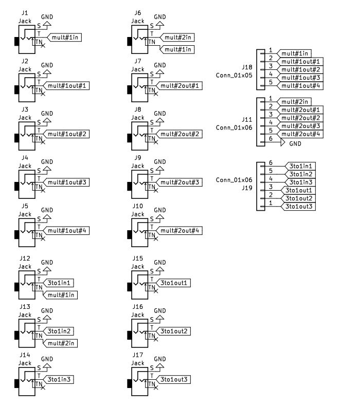
 JACK BOARD BOM Qty 
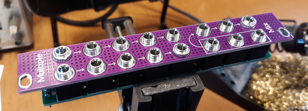
16 J1, J2, J3, J4, J5, J6, J7, J8, J9, Thonkiconn or compatible jack. Tayda Part# A-2563 J10, J12, J13, J14, J15, J16, J17 2 J11, J19 Male 1x6 header, 2.54mm pitch 1 J18 Male 1x5 header, 2.54mm pitch Notes: The 10 Ohm resistors R11 and R12 could be substituted with diodes for reverse voltage protection, or polyfuses or ferrite beads, or just a jumper link, depends on your personal philosophy about such protection for the power rails. You can try different TL07x compatable pinout op amps to see if you like them better, like TL08x, etc. 33K Ohm resistor, R16 could be tweaked depending on the size of the signals you are mixing and what effect you want for attenuation or amplification. All caps best rated 25V or higher. If you get confused, listen to the music play. Then email me. |
![]() |
Resistors go vertically. |
![]() |
I Don't pay any attention to the size of the silk circles where the resistors go in respect to the bent lead, I place them so soldering is easy. |
![]() |
I solder the bent lead from the top side then flip and solder the other lead from the bottom. (notice the little solder blob on the blurry resistor lead in the back - I cleaned that up) |
![]() |
The electrolytic caps need to fit, so I choose short enough ones or put them on the back side. Next revision I'll put the cap silkscreen on both sides. |
![]() |
I use sockets for the ICS. |
![]() |
You can see how tall the caps can be when I put the male & female headers together for soldering the sandwich. |
![]() |
I Solder the jack board to the male headers.then flip and solder the mainboard, keep it all together so it aligns. |
![]() |
I Place all the Thonkiconn style jacks... |
![]() |
I Put the panel on with a couple of the nuts in place. |
![]() |
I Carefully flip over holding it together and solder the jacks. It's easy to bobble and will make you sad when you have to place the jacks all over again. |
![]() |
I test the power rails of the sockets to make sure voltage goes where it should. I use sockets. I mean you could solder the opamps directly but why? |
![]() |
I put in the ICs. |
![]() |
And squeeze it all together. If Im feeling insecure I put a dab on hot glue on the headers after it's all tested so it doesn't come loose over time. |
![]() |
Testing... |
![]() |
Looks like a nice copy. |
![]() |
2 to 1 mix. |
![]() |
Light blue is the mixed signal. |
![]() |
Three inputs, top is mixed signal. Looks like shorthand. |
![]() |
Same but different waveforms. |
![]() |
This is my testing setup... |